
Printed Circuit Board (PCB) Design Summer School: Session 2 of 4
Join us for Maker Summer School! In this summer series, you can learn how to design your own printed circuit board using the free open source (FOSS) software package KiCad.
Over four evening sessions, fablab|nk manager Graham will take you on a gentle dive into the typically hidden-world of everyday electronics and help you start to make your own.
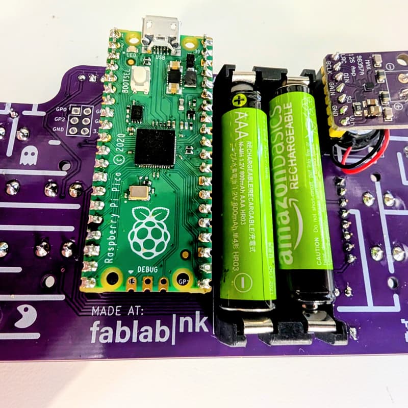
From LED 'blinky' badges to, mini-keyboards and games-consoles, circuit-board jewelry and synthesisers - we'll take a look at a series of example projects that we’ve produced over the last year and use those as jumping-off points for your own designs. So whether you're a budding hardware engineer or an artist looking explore a new fabrication technique - you'll find the practical tools you need here.
And of course we’ll learn some electronics too as a side effect :)
Note: While it's possible to join for any of the sessions to get a taste, to fully produce a finished-board of your own design you should plan to attend all four. All sessions will be held in English.
17.06 Session 1: The Printed Circuit Design Workflow
Trip to China: Virtual tour of a PCB factory
“Hello Hardware World”: laying out, checking and uploading a minimal first design
Components and Their Footprints: through-hole vs surface mount
Overview of starter projects
24.06 Session 2: Deeper-Dive into Schematics and Boards
How to create a schematic (and re-use those of others)
Performing an electrical rules check (ERC)
From schematic to board: board shape, footprints and layouts (DRC)
Assisted individual project time
01.07 Session 3: Individual Projects and Advanced Topics
Traces vs pours and other routing tips-and-tricks
"Round-tripping" for artistic PCB design: from KiCad to Inkscape and back
Case study: Designing to mill-it-yourself (MIY) on our CNC mill
How to make your own custom symbol and footprints
Assisted individual project time
08.07 Session 4: Advanced Topics and Ordering
Big push to complete and order your designs!
Design options: beyond 2-layer boards and rigid PCBs
Case study: Fully-assembled PCBs (e.g. butterfly project)
Fabrication with JLCPCB: tips and tricks